Flashy RAM for the anime enthusiast
By now, it’s common knowledge that Intel’s 12th Generation Alder Lake will be the first mainstream processor platform to embrace DDR5 memory. The chipmaker (via momomo_us) has released a new document that lists the different DDR5-4800 memory modules that have been validated for its next-generation platform.
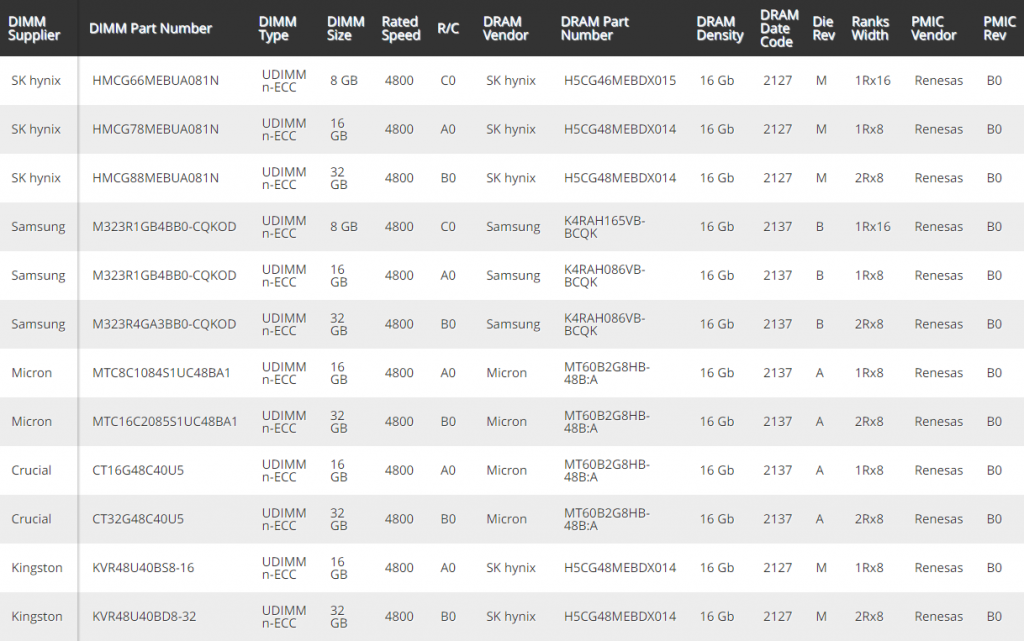
Instead of validating the different DDR5 products itself, Intel delegated the arduous task to Advanced Validation Labs, Inc (AVL), a renowned specialist in testing and validating memory during the pre- or post-production phase. The company specifically concentrated on DDR5-4800 memory, which is the baseline standard for Alder Lake. These are non-ECC memory modules that stick to JEDEC’s guidelines, including a 1.1V DRAM voltage and mediocre 40-39-39 timings.
AVL tested memory modules from big-name vendors, such as SK hynix, Sasmsung, Micron, Crucial and Kingston. While the data rate remains the same for all the candidates, the capacities vary between 8GB and 32GB per memory module. According to the Intel document, DRAM manufacturers will start with 16-gigabit DDR5 RAM chips. so there’s enough headroom to work up to the capacity that they want to offer for each individual memory module.
One of the novelties with DDR5 is the onboard voltage regulation, which is achieved by equipping the memory module with a power management integrated circuit (PMIC). As far as the initial DDR5 memory modules are concerned, they’ll leverage a PMIC from Renesas. The document didn’t specify the exact model of the PMIC. However, we think it might be the P8911, which is an optimized version of the P8900 that Renesas designed for server memory.
DDR5-4800 Specifications
SK hynix, Samsung and Micron are IC manufacturers, so naturally they’ll utilize their own ICs in their DDR5 products. Kingston, on the other hand, will tap SK hynix for its ICs/ Meanwhile Crucial, which is Micron’s consumer brand, will utilize the latter’s ICs.
If we look at the ICs, it would seem that SK hynix and Micron will be bringing their respective M-die and A-dies to DDR5. These scale good enough with higher voltages, but they aren’t exactly recognized for operating with tight timings. That’s where Samsung’ B-die ICs excelled back in the DDR4 days. The document confirms that Samsung’s DDR5 ICs are Revision B, so these should be B-die. If the DDR5 B-dies are anything like the previous DDR4 B-dies, they’ll probably become the de facto ICs for overclockers again.
Apparently, the recipe doesn’t vary with 8GB and 16GB memory modules, regardless of the brand. The companies will stick with a single-rank design, 1Rx16 for 8GB and 1Rx8 for 16GB. In comparison, 16GB DDR4 used to be a guarantee for dual-rank in the beginning. Eventually, many memory brands have transitioned to a single-rank design thanks to the introduction of higher-density chips. With DDR5, however, 32GB memory modules are the only surefire ticket for a dual-rank (2Rx8) layout.
Why does the above matter? Dual-rank memory is typically faster than single-rank memory, although not in all workloads. Both Intel’s Core and AMD’s Ryzen processors benefit from dual-rank memory, and tests have shown that four memory ranks is the ideal configuration for maximum performance. It remains to be seen whether Alder Lake favors the same setup, though.

