Intel revealed three new packaging technologies at SEMICON West: Co-EMIB, Omni-Directional Interconnect (ODI) and Multi-Die I/O (MDIO). These new technologies enable massive designs by stitching together multiple dies into one processor. Building upon Intel’s 2.5D EMIB and 3D Foveros tech, the technologies aim to bring near-monolithic power and performance to heterogeneous packages. For the data-center, that could enable a platform scope that far exceeds the die-size limits of single dies.
The focus of semiconductors is usually on the process node itself, but packaging is one of the oft-unsung enablers of modern semiconductors. Ultimately a silicon chip is just part of a bigger system that requires power and data interconnection. Packaging, in that view, provides the physical interface between the processor and the motherboard – the board acts as a landing zone for the chip’s electrical signals and power supply. Intel stated a few years ago that its assembly and test R&D is bigger than the top two OSATs (outsourced assembly and test) combined.
Packaging innovation could lead to smaller packages that enable bigger batteries as we had seen with Broadwell-Y. Similar board size reductions have been realized with the use of interposers to integrate high-bandwidth memory (HBM). With the industry tending towards a heterogeneous design paradigm with chiplet building blocks, the platform-level interconnect has gained greatly in importance.
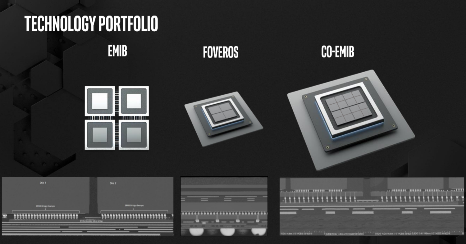
EMIB
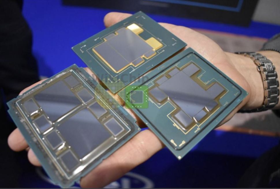
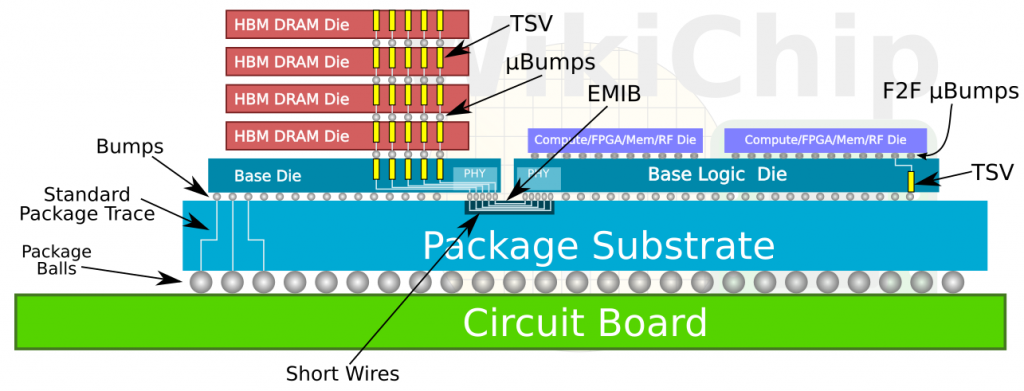
Intel has been shipping its EMIB (Embedded Multi-die Interconnect Bridge), a low-cost alternative to interposers, since 2017, and it also plans to bring that chiplet strategy to its mainstream chips. In short, EMIB is a silicon bridge that enables a high-speed pathway between two chips. The bridge is embedded inside the package between two adjacent dies.
Compared to interposers, which can be reticle-sized (832mm2) or even larger, EMIB is just a small (hence, cheap) piece of silicon. It provides the same bandwidth and energy-per-bit advantages of an interposer compared to standard package traces, which are traditionally used for multi-chip packages (MCPs), such as AMD’s Infinity Fabric. (To some extent, because the PCH is a separate die, chiplets have actually been around for a very long time.)
Another advantage of EMIB is the ability to build each function or IP block of a chip on its own most-suitable process technology, which reduces costs and improves yield by using smaller dies. EMIB has several other advantages, such as decoupling IP development and integration by allowing designers to build chips from a library of chiplets, using the best chiplet available at each point in time. Intel currently uses EMIB in the Stratix 10, Agilex FPGAs, and in Kaby Lake-G, and the company has more extensive plans for the technology on its roadmap.
Foveros
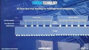
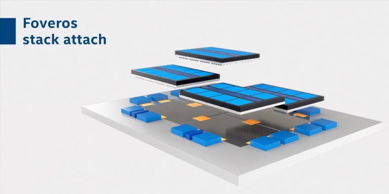
At its Architecture Day last year, Intel went a step further, describing its upcoming 3D Foveros technology that it will use in Lakefield. To recap, it is an active interposer that uses through-silicon vias (TSVs) to stack multiple layers of silicon atop each other. It has even lower power and higher bandwidth than EMIB, although Intel hasn’t discussed their relative cost.
In Lakefield, Foveros is used to connect the base die (which provides power delivery and PCH functionality) on 22FFL to the 10nm compute die with four Tremont and one Sunny Cove core. In May, the company teased its vision of an advanced concept product using both EMIB and Foveros together to an create enormous package with many chips, all on a single package.
On Tuesday at SEMICON West, Intel unveiled three more advanced packaging technologies it is working on.
Co-EMIB
Co-EMIB is the technology that will largely make the above heterogenous data-centric product a reality. In essence, it allows Intel to connect multiple 3D-stacked Foveros chips together to create even bigger systems.
Intel showed off a concept product that contains four Foveros stacks, with each stack having eight small compute chiplets that are connected via TSVs to the base die. (So the role of Foveros there is to connect the chiplets as if it were a monolithic die.) Each Foveros stack is then interconnected via two (Co-)EMIB links with its two adjacent Foveros stacks. Co-EMIB is further used to connect the HBM and transceivers to the compute stacks.
Evidently, the cost of such a product would be enormous, as it essentially contains multiple traditional monolithic-class products in a single package. That’s likely why Intel categorized it as a data-centric concept product, aimed mainly at the cloud players that are more than happy to absorb those costs in exchange for the extra performance.
The attraction is that the whole package provides a near-monolithic performance and interconnect power. Additionally, the advantage of Co-EMIB over a monolithic die is that the heterogeneous package can far exceed the monolithic die-size constraints, with each IP on its own most suitable process node. At its Investor Meeting in May, Chief of Engineering Murthy said Foveros would allow the company to intercept new process technologies up to two years earlier by using smaller chiplets.
Of course, since EMIB is a bridge inside the package, it is inserted at the start of the assembly process, followed by the Foveros stacks. WikiChip has provided a diagram of Co-EMIB used to connect two Foveros stacks.
ODI
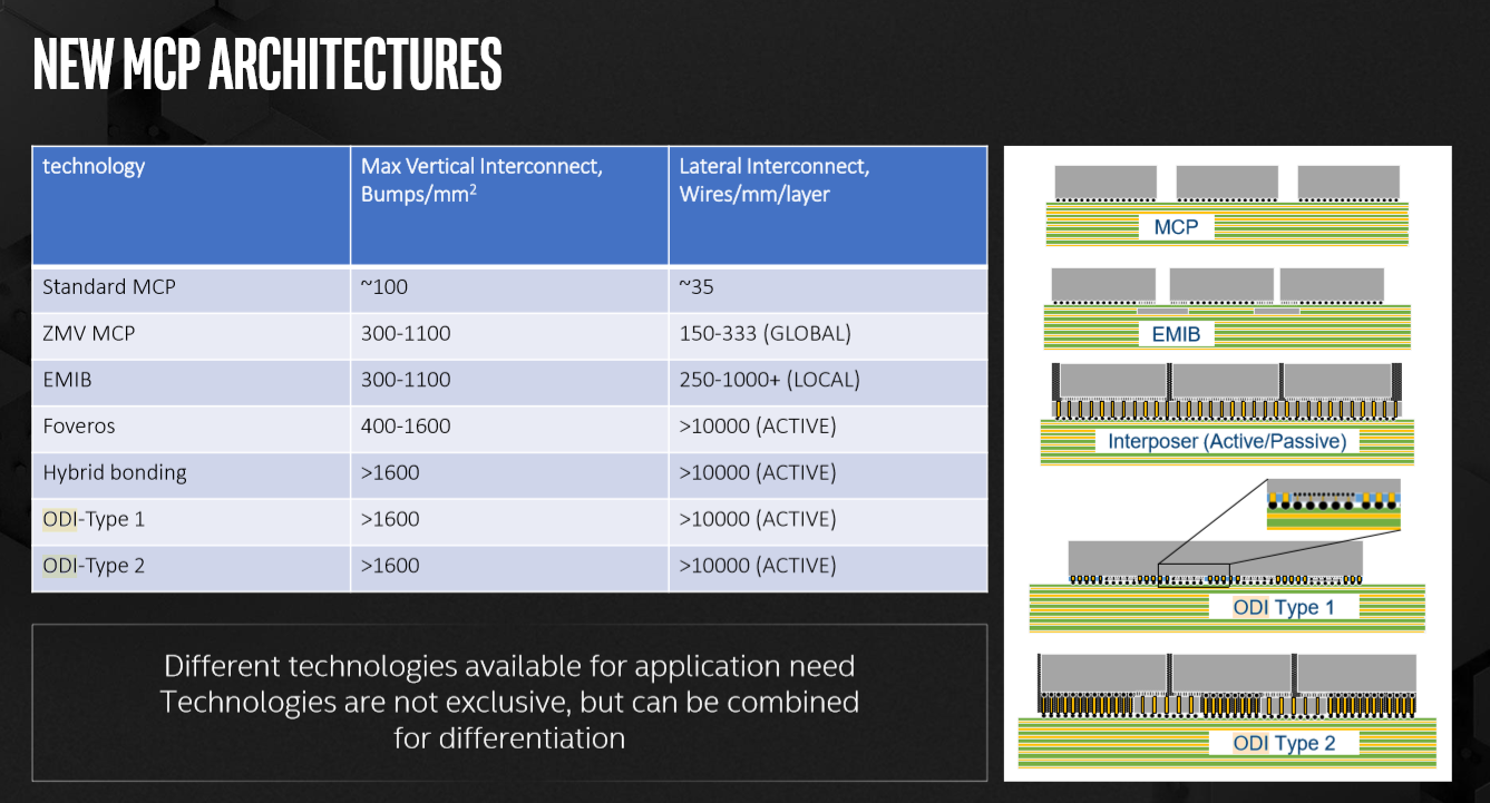
Omni-Directional Interconnect (ODI) is a new interconnect. It is yet another type of multi-chip interconnect besides the standard MCP, EMIB, and Foveros. As the name implies, it permits both horizontal and vertical transmission. The bandwidth is higher than traditional TSVs because the ODI TSVs are much larger. This allows for current conduction directly from the package substrate. Resistance and latency are also lower. ODI will need far fewer vertical channels in the base die than traditional TSVs. This minimizes the die area and frees up area for active transistors.
MDIO
Lastly, Multi-Die I/O (MDIO) is an evolution of the Advanced Interconnect Bus (AIB) that provided a standardized SiP PHY-level interface for EMIB, for chiplet-to-chiplet communication. Last year, Intel donated its AIB to DARPA as a royalty-free interconnect standard for chiplets. MDIO bumps up the pin speed from 2Gbps to 5.4Gbps. The areal bandwidth density has increased somewhat, but mainly the linear bandwidth density has increased by a large factor. Intel reduced the I/O voltage swing from 0.9V to 0.5V and improved energy efficiency. Intel also provided a comparison to TSMC’s recently announced LIPINCON.
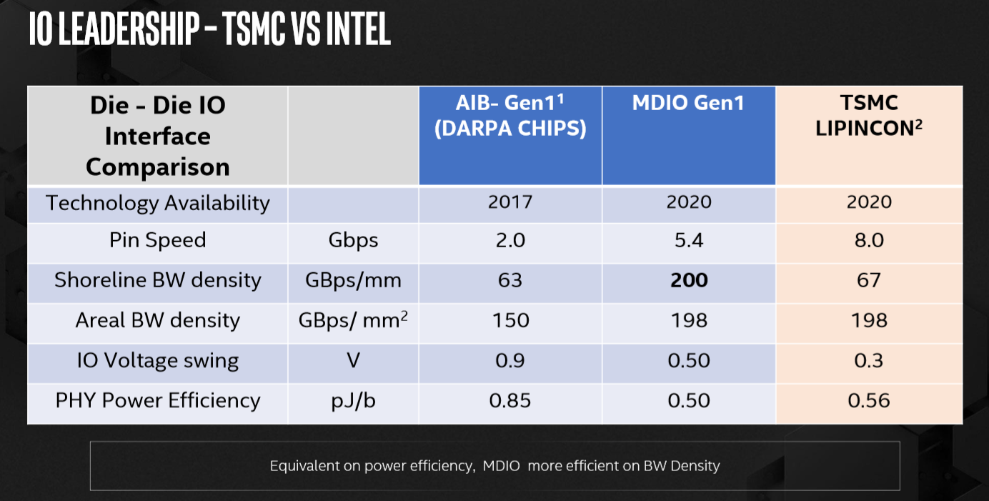
One word of caution, though. While it would seem that a higher pin speed it better, that is not necessarily the case, higher speeds tend to result in higher power consumption. It’s best to look at it is as a whole spectrum of interconnect options. At one end of the spectrum, there are protocols with high lane speeds (and hence, few lanes), such as PCIe 4.0’s 32Gbps. At the other end, technologies such as EMIB and HBM have a lower per-pin data rate, but typically they have many more interconnections. EMIB’s roadmap consists of shrinking the bump pitch, which will provide ever more connections, so a high lane rate isn’t a priority.
Further Discussion
When they are ready, these technologies will provide Intel with powerful capabilities for the heterogeneous and data-centric era. On the client side, the benefits of advanced packaging include smaller package size and lower power consumption (for Lakefield, Intel claims a 10x SoC standby power improvement at 2.6mW). In the data center, advanced packaging will help to build very large and powerful platforms on a single package, with performance, latency, and power characteristics close to what a monolithic die would yield. The yield advantage of small chiplets and the establishment of chipset ecosystem are major drivers, too.
As an Integrated Device Manufacturer (IDM), Intel says it can extensively co-develop its IP and packaging in a way that no other company could possibly do, from silicon to architecture and platform. As Babak Sabi, CVP of Intel’s Assembly and Test Technology Development, put it: “Our vision is to develop leadership technology to connect chips and chiplets in a package to match the functionality of a monolithic system-on-chip. A heterogeneous approach gives our chip architects unprecedented flexibility to mix and match IP blocks and process technologies with various memory and I/O elements in new device form factors. Intel’s vertically integrated structure provides an advantage in the era of heterogeneous integration, giving us an unmatched ability to co-optimize architecture, process, and packaging to deliver leadership products.”
MDIO is slated for 2020 availability. Rumor has it that Intel is going to use Foveros, and hence possibly Co-EMIB, with Granite Rapids in early 2022. Intel has not specified a timeframe for ODI.