Micron announces impressive 1α fabrication process for DRAM.
Micron on Tuesday announced its new 1α fabrication process for DRAM. Initially, the company will use it to make DDR4 as well as LPDDR4 memory, but over time it will be used to produce all types of the company’s DRAM. The manufacturing technology promises tangible increases in DRAM density and reduces costs, but the company warns that it is getting exceedingly hard to scale DRAM.
New Technology for New DRAMs
By now, Micron has transited a substantial part of its DRAM production to its 1Z nm node that offers both high bit density (i.e., lower costs per bit) and high performance (i.e., enables higher margins). As a result, right now Micron says it feels rather comfortable in terms of profit margins and product mix. Micron’s 1α fabrication process is projected to offer a 40% improvement in bit density compared to 1Z (at mature yields), which will decrease the producer’s costs per bit accordingly.
In addition, the technology is said to feature a 15% drop in power consumption as well as higher performance. One of the important aspects about Micron’s 1α is that, roughly, 10% out of its 40% bit density improvement over the predecessor is driven by DRAM design efficiency, which shows that lithography improvements alone are not enough to make DRAM cheaper to build. Micron’s 1α node continues to use 6F2 bit line design, just like its predecessors. Nonetheless, the company has implemented numerous innovations to shrink its DRAMs with the latest fabrication process.
“The strong improvement on 1-alpha bit density is driven by combination of process technology improvement, as well as very strong improvement in array efficiency due to design improvements,” said Thy Tran, Micron vice president of DRAM process integration. “Array efficiency alone gave us approximately 10% of the design improvement. In addition, we had strong process technology improvement. To accomplish this, an aggressive shrink of the bitline and wordline pitches was needed — shrinking the grid, so to speak. To do that, we were much more aggressive than before in implementing the new processes. We’re incorporating the latest and greatest everywhere: new materials – better conductors, better insulators, new machinery to deposit, modify or selectively remove – etch – those materials. Shrinking these pitches in turn resulted in more aggressive scaling of the cell capacitor, which required innovations to meet the structural and electrical requirements. Additionally, we also introduced advanced tools and novel techniques to improve the alignment of one patterned layer to another.”
Pathfinding for the new technology mostly took place in Micron’s headquarters in Boise, Idaho. But the process development and manufacturing ramp involved numerous global teams working closely between the U.S., Taiwan and Japan.
“Our new 1α DRAM technology will enable the industry’s lowest-power mobile DRAM as well as bring the benefits of our DRAM portfolio to data center, client, consumer, industrial and automotive customers,” said Sumit Sadana, executive vice president and chief business officer at Micron.
Initially, Micron will use its 1α node to make 8Gb and 16Gb DDR4 and LPDDR4 memory chips at its Taiwanese fabs in Taoyuan and Taichung, but eventually use of the technology will be expanded to other types of memory. Technologies like 1α will be particularly useful for next-generation DDR5 memory devices that will feature a more complex architecture compared to today’s DRAMs.
“Our 1α node will be gradually deployed across our product portfolio and will be our workhorse in fiscal 2022,” said Ms. Tran. “We will transition our fabs gradually to grow our production in line with the industry demand.”
Scalability Challenges
Memory technologies have evolved greatly in recent years, as the industry needed considerably higher performance. Modern and upcoming interfaces — such as DDR5 and GDDR6X — are considerably more complex than DDR4 and or GDDR6, which is why it is harder to scale modern DRAMs. But the emergence of technologies like DDR5 and GDDR6X is something inevitable, so going forward companies like Micron will need to invest more in the engineering of process technologies.
“There is a constant demand for higher performance and we are able to deliver this through process and design innovations,” said Naga Chandrasekaran, Micron senior vice president of technology development. “DDR5 actually enables the performance requirements while we scale for cost. DDR5 can reduce power consumption and provide higher bandwidth. At the same time, such high-performance requirements place some challenges with respect to die size that cannot be compensated by dimensional scaling alone. So, delivering higher performance requirements while delivering cost reduction is extremely challenging and requires innovations from multiple vectors beyond process solutions.”
Since modern DRAM process technologies have to get thinner (as they cannot scale vertically, unlike 3D NAND), challenges for companies like Micron are not getting any simpler. as the company has to find the right balance between cost, performance, quality, and power.
“DRAM scaling continues to become even more challenging, especially when we have to battle extremely tight process margins, while optimizing for cost, power and performance, as well as quality,” said Mr. Chandrasekaran. “While we are trying to deliver improved performance, we are also constantly challenged to improve cost, which drives dimensional scaling. This scaling challenge has always been there and continues to become harder as the aspect ratio increases. To meet increasing demand for performance/power, we have to implement advanced process solutions, which can be expensive. As we scale to reduce cost, performance/power can be challenged due to device limitations, which in turn drive the need for advanced processes that can drive cost higher. So, balance between cost/performance-power requires solutions beyond just process scaling and solutions.”
One of the ways to solve geometry scaling challenges is to adopt extreme ultraviolet (EUV) lithography, but that is not something that Micron plans to do for several years to a large degree, because EUV does not solve all the tasks that DRAM makers face these days.
No EUV for Micron, for Now
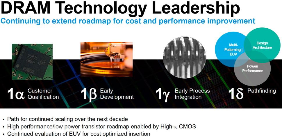
Unlike its industry peers, Micron Technology does not plan to use EUV lithography to produce memory in the short-term future, but intends to rely on all kinds of multi-patterning. Micron’s next three DRAM nodes will continue to use deep ultraviolet (DUV) lithography, but the company is now considering to use EUV for its 1𝛿 fabrication process. Meanwhile, even without EUV, Micron promises performance and power improvements for its next-gen memory devices, though the company admits that it is getting harder to shrink DRAMs.
“We need constant innovation in materials, process, and equipment to meet scaling needs,” said Mr. Chandrasekaran. “We are implementing several such solutions in our current and future technologies. With respect to EUV, as we have highlighted, our proprietary and innovative multi-patterning technology is able to meet our performance and cost requirements. Through our process solutions and advanced control capability, we are able to meet the technology node requirements.”
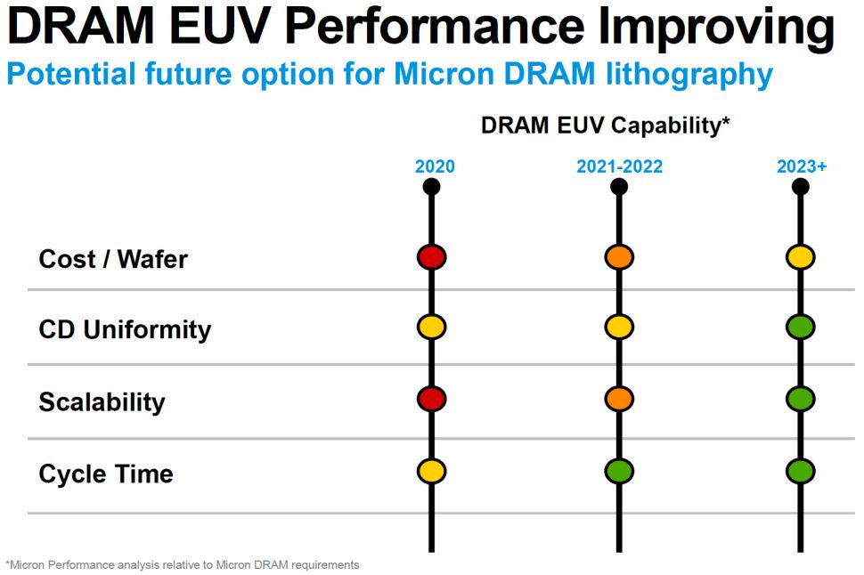
Micron believes that in the coming years, improvements brought by EUV-enhanced manufacturing technologies will be offset by costs of equipment and difficulties with production as EUV is still in its early stages as far as DRAM production is concerned. For example, a slide recently demonstrated by Micron indicates that EUV costs are prohibitively high, scalability advantages are negligible, critical dimension (CD) uniformity is not perfect (which may affect quality and performance), whereas cycle times are not reduced significantly because the productivity of EUV scanners is still behind that of DUV scanners.
“The current EUV tools are not at similar capability as the advanced immersion technology,” said Micron’s senior vice president of technology development. “While improvements are being made with EUV technology, their cost and performance still lag behind current multi-patterning and advanced immersion capability. We are constantly evaluating EUV and believe that over the next three years EUV will make the required progress to compete on cost and performance with advanced pitch multiplication and immersion technologies. Micron is evaluating EUV and will introduce it at the right time when it meets our requirements.”
As a result, Micron’s 1β, which is in development, and 1𝛾 nodes will not employ any EUV layers. Instead, the company will continue to use multi-patterning and will task its engineers to design as efficient DRAMs as possible to ensure that its devices are competitive in terms of bit density, power, and performance.
Assuming that Micron introduces a new fabrication process roughly every year, like DRAM makers have been doing in the recent years, its 1𝛿 node is due sometime in 2024 or later. Introducing EUV four years after Samsung, the world’s largest maker of memory, has pros and cons. On the one hand, Micron will use perfected EUV tools, mask pellicles, and resists. On the other hand, it will have to introduce EUV across multiple layers without having any experience with high volume manufacturing (HVM) using EUV.


